

Cytech is pleased to offer FPGA training course in Beijing, Shanghai and Shenzhen office. The Q2 and Q3 training arrangement are below:
| Time | Location | Telphone | |
|---|---|---|---|
| 2013-5-9 | Shanghai | samhu@cytech.com | Tel:(021) 6440 1373 |
| 2013-7-19 | Beijing | Nancyhuang@cytech.com | Tel:(010) 8260 7990 |
| 2013-5-21 | Shenzhen | karldli@cytech.com | Tel:(0755) 2693 5811 |
| 2013-8-29 | Shanghai | samhu@cytech.com | Tel:(021) 6440 1373 |
| 2013-10-18 | Beijing | Nancyhuang@cytech.com | Tel:(010) 8260 7990 |
| 2013-9-24 | Shenzhen | karldli@cytech.com | Tel:(0755) 2693 5811 |
| 2013-10-17 | Shanghai | samhu@cytech.com | Tel:(021) 6440 1373 |
| 2013-11-15 | Beijing | Nancyhuang@cytech.com | Tel:(010) 8260 7990 |
| 2013-11-21 | Shenzhen | karldli@cytech.com | Tel:(0755) 2693 5811 |
The course include below modules:
| A. Basic Course | B. Optimize Course | C. Application |
|---|---|---|
|
|
|
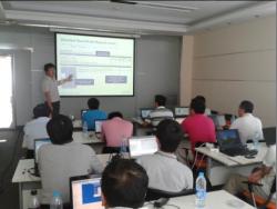
Some course have lab and will use EasyGX dev kit. The training location is Cytech Shanghai, Shenzhen and Beijing training room. The attendee need to bring their own notebook and install related software in advance.
 |
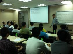 |
| 2012 Q3 Timing analysis course in Shanghai | 2013 Q1 Design optimize course in Shenzhen |