

When a large FPGA is used, the amount of current that the FPGA requires from the power supply increases. As a result, the RMS current flowing through the power supply input line increases.
What if the input RMS current increases?
When the RMS current flowing into the input section of the DC / DC converter increases, the switching noise in the input section increases.
You may not have noticed the RMS current at the input before, but if the current value used in the FPGA increases in the future, you will need to review it.
Let‘s think about it using the DC/DC converter named LTM4650A-1 in Figure 1.
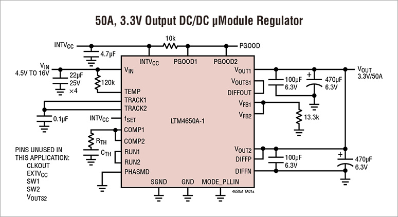
Figure 1: LTM4650A-1 Circuit diagram
LTM4650A-1 contains two 25A output DC/DC converters.
The 2 channel DC/DC outputs can be combined into a single connection for 50A output.
Even with 50(A), a high efficiency of approximately 95% has been achieved (Figure 2).

Figure 2: LTM4650A-1 efficiency curve
In general, the input RMS current for a single output is as shown in Figure. 5.
Dual input currents IIN 1 and IIN 2 add up to a large RMS current.
Large RMS current appears as switching noise.
This RMS current noise can also cause system malfunction.
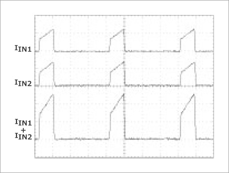
Figure 3 : Single-Phase RMS Current Waveform
Now let’s calculate the RMS current using the following equation.
Assuming that the input is 12V, the output is 1.0V and the maximum current is 50A, the efficiency is approximately 87% from Figure. 1.
When calculated, the RMS current value is approximately 16A.

η%:Estimated efficiency of the power supply module
D: Duty cycle of the step-down converter
D = VOUT / VIN
Two-phase operation to suppress RMS current as noise source
The two-phase operation changes the switching timing of the switching regulator 1 and 2 in the LTM4650-1 by 180 degrees.
As shown in Fig. 4, when the phase of the input current IIN 1 of the regulator 1 and that of the input current IIN 2 of the regulator 2 are shifted by 180 °, the frequency increases by a factor of 2, but the maximum value of the input current becomes half of that in the single phase operation.
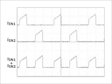
Figure 4 : Two-Phase Operation Waveforms
This reduces switching noise on the input line, making it easier to take measures against EMI compared to the single phase, and reducing the impact of system problems caused by noise.
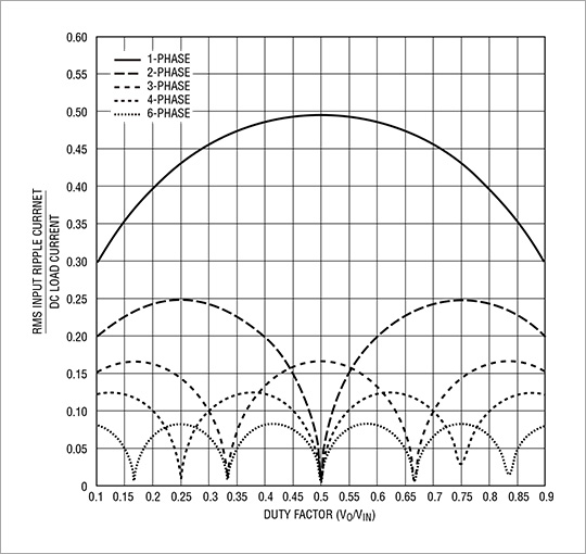
Figure 5 : Normalized Input RMS Current for Two-Phase Operation
From the normalized input RMS current graph shown in Fig. 5, estimate the RMS current during the two-phase operation. If the duty is approximately 0.1, the ratio of RMS / Maximum Current is 0.2.
As a result, the Two-Phase RMS current is approximately 10A, which is much less than the Single-Phase RMS current of 16A.
This greatly reduces the switching noise that appears on the input line.
Reduction of input ceramic capacitors
In addition to reducing the switching noise on the input line by reducing the RMS current, there is another benefit.
Ceramic capacitors can be reduced.
Generally, the self-heating value of ceramic capacitors should be kept below 20℃.
Therefore, as the RMS current increases, the self-heating increases, so it is necessary to increase the number of capacitors to disperse the self-heating.
Assumed that a ceramic capacitor with an RMS current value of 4.2A and self-heating 20℃ was used.
The number of ceramic capacitors required for single and dual phase operation are
⦁ Single Phase:4(16A ÷ 4.2A = 3.81)
⦁ Two Phase:3 (10A ÷ 4.2A = 2.38)
Since there are so many ceramic capacitors on the FPGA board, reducing the number of ceramic capacitors even by 1 is a manufacturing advantage in terms of reduced implementation and administrative costs.
| Back to Technical Articles |
| Contact us |