

Using Cyclone10LP device to achieve data recovery of serial communication
For non-source synchronous low-speed serial data communication scenarios, there would be a situation that the clock frequency of the opposite end of the communication is relatively different, as a result, data receiver could not sample correctly. In this case, using Altera’s high-end devices like high-speed transceiver or LVDS SerDes’ SOFT-CDR and DPA function can solve the problem. However, low-end devices like Cyclone IV or Cyclone 10LP are not equipped with transceiver, and the corresponding LVDS SerDes are not equipped with SOFT-CDR and DPA function as well. Therefore, the data recovery of serial communication could only be achieved by our own designed logic.
The technique of the design, is doing 8 times oversampling for the received data, by both rising and falling edge of the receiving end’s reference clock that with a phase shift of 0 ° and 90 °, then choosing a stable value for clock domain by logic judgement, and using the clock domain sampling data as reliable data.
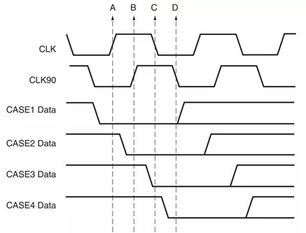
Image 1
In image 1, the first trigger is sampled by clock domain A (CLK rising edge), the second trigger is sampled by domain B (CLK90 rising edge), the third trigger is sampled by domain C (CLK falling edge), and the forth trigger is sampled by domain D (CLK90 falling edge).
To eliminate metastability, four-level sampling is needed for the 4 triggers, instead of one level sampling. See image 2:
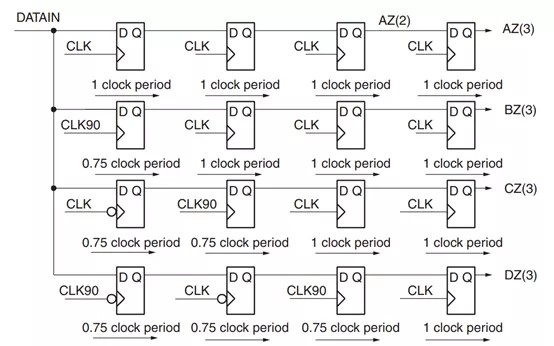
Image 2
According to image 2, after sampling the triggers step by step, level 3 triggers are named as AZ(2), BZ(2), CZ(2), & DZ(2), and level 4 triggers are named as AZ(3), BZ(3), CZ(3), & DZ(3).
After the four-level sampling of the four clock domains, a combinatorial logic is needed. See image 3:
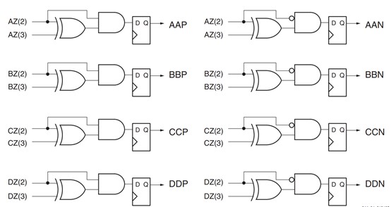
Image 3
After working on logic XOR, AND / NAND according to image 3, data described as AAP, AAN, BBP, BBN, CCP, CCN, DDP, and DDN are obtained through the triggers.
Then, a reliable clock domain decision is needed, that means choosing the clock domain with the most stable sampling data:
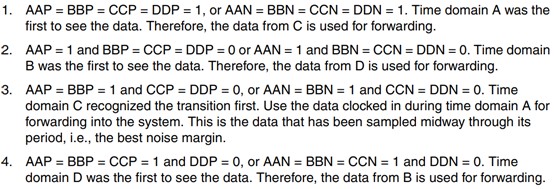
In reality, engineers may face situations like: the clock frequency of data transmitting source is 401MHz, while the clock frequency of data receiving end is 400MHz, or in opposite, the clock frequency of data transmitting source is 400MHz while clock frequency of data receiving end is 401MHz. Through simulation, the result after logical decision would be changed periodically (that means the stable clock domain may change from D to A after a period of time). But it doesn’t matter. According to its decision as the most reliable clock domain to do the sampling, the data obtained should be correct.
As the clock domain judgment result would be changed, the design of a short logic is needed for data filtering. See image 4:
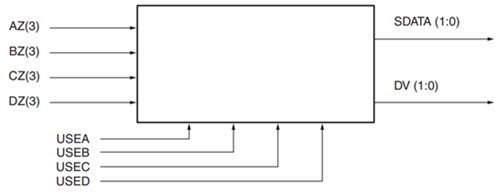
Image 4
The target of the design above is to find out the most reliable clock domain which could stable data sampling. Though the clock domain might be changed because of the communication clock frequency deviation, the sampled data would still be stable and reliable. At present, for one of our customers, a verification data serial communication based on 10CL010YU256C8G and 10CL016YU256C8G, and a long time on-hook testing for PRBS communication are applied on its hardware basics. And the bit error ratio is 0.
The customer’s related products have been mass produced. And for sure, for better quality of communication, codec module 8B10B is needed in actual product.